Multiscale Mask-less Laser Lithography
-
Offering type ?
PRODUCT:
Component or system, which is commercialized. It is available for ordering multiple pieces and liability is assumed by the provider/seller. Necessary certification of the product was obtained (e.g. CE certification). The product sheet and/or conditions of use are defined.
PROTOTYPE:
Component or system, which has been successfully tested under real or real-like conditions. The prototype is not commercialized as the main purpose is to use it for demonstration and experimentation, including user and market acceptance.
TECHNICAL SERVICE:
Tools and processes and its combination, which are necessary to prepare and test prototypes or products.
- Prototyping
- Masters (origination)
- Service
-
Market
- AR/VR/MR
- Automotive
- Lighting
- Optical instrumentation
- Security & Branding
-
Manufacturing Pillar
- Roll-2-Roll
-
Technology
- Laser Lithography - Maskless
Offering Description
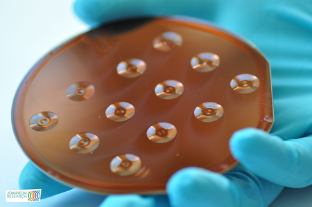
Origination by mask-less Laser Lithography
Our unique mask-less laser lithography enables the low-cost production of novel and complex high-resolution sub-micro and micro-structures:
- Master fabrication e.g. for UV-nanoimprint lithography, hot-embossing, high precision optical injection moulding, vacuum resin casting
- a Rapid prototyping in Micro-Optics, Photonics, Microfluidics, Electronics and others
Several advantages can be realised:
- Reduction of process time
- digital, non-photomask-based production
- quick and flexible to test and implement design changes
- fabrication of microstructures on flat and curved substrates via 5-axes nano-positioning system
Applications can be found in
- Free form micro optics for innovative illumination designs
- Diffractive and refractive micro optical elements
- Bionic surfaces in aviation for reduction of drag to reduce fuel consumption
- Microfluidic Lab-on-Chip systems for molecular diagnostics
- Micro-Electronics
Offering Specifications
- High quality fabrication of sub-micro and micro-structures on large area formats (2″, 4″, possibly 6″ substrate)
- Structures can have a 1D, 2D, or stepless (2.5 D) relief shape
- Minimum structure size achieved in the lateral direction of our system is in the range of 300 nm
- Maximum structure depth for 2.5D microstructures is in the range of 80 μm
- Aspect ratio of 4 is possible
- Depending on the complexity of the designed microstructure, the processing time is approx. 1 hour per cm2