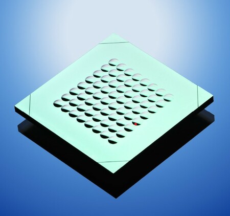
Etched Microlenses
-
Offering type ?
PRODUCT:
Component or system, which is commercialized. It is available for ordering multiple pieces and liability is assumed by the provider/seller. Necessary certification of the product was obtained (e.g. CE certification). The product sheet and/or conditions of use are defined.
PROTOTYPE:
Component or system, which has been successfully tested under real or real-like conditions. The prototype is not commercialized as the main purpose is to use it for demonstration and experimentation, including user and market acceptance.
TECHNICAL SERVICE:
Tools and processes and its combination, which are necessary to prepare and test prototypes or products.
- Volume production
-
Market
- Imagers & Displays
- Optical instrumentation
-
Manufacturing Pillar
- Wafer-scale
-
Technology
- Dry Etching
- Thermal Reflow
- Photolithography
- Other
Organisation
Offering Description
Focuslight is committed to providing the highest quality components underpinned by cutting edge manufacturing techniques. Combined with a unique blend of people skills, its innovative advances in technology make Focuslight a leader in its product offerings.
Focuslight provides a broad range of customized microlenses for efficient collimation and light coupling for fiber optics, as well as Si-Photonics, PIC, WSS, laser diodes, VCSEL, CWDM, DWDM and more. These MLA’s can be used for the visible and infrared applications.
KEY FEATURES
+ 1D & 2D microlens arrays + Highest quality and precision + Bulk material: fused silica, silicon, borofloat + Wavelength range: DUV to Mid-IR + Lens profile: sphere, asphere + Sub-micron position accuracy
ADDITIONAL FEATURES
+ Trenches for glue stops and glue pockets, pupils, pinholes, alignment marks, mounting posts + Double-sided lens arrays with precise frontto-back alignment + AR coating, metallization, wafer-level packaging + Wafer thinning
Offering Specifications
- Materials: Fused silica (various grades), silicon
- Numerical aperture (NA) – Typically 0.09 to 0.6
- Mode Field Diameter (MFD) – 0.6 μm to 50 μm
- Beam Diameter/Output – 50 to 400 µm, others on request
- Fiber/Waveguide types – SMF, MMF, LD, PIC,
- Si-Photonics Back focal distance – Typically 0 to 300 μm
- Pitch – 82 μm, 125 µm, 250 µm, 500 µm, 750 µm, and custom pitch
- Lens type – Circular, cylindrical
- Lens profile – Spherical, aspheres, DOE
- Arrays Linear, quadratic, hexagonal, custom


