Microimprint on Wafer Level
-
Offering type ?
PRODUCT:
Component or system, which is commercialized. It is available for ordering multiple pieces and liability is assumed by the provider/seller. Necessary certification of the product was obtained (e.g. CE certification). The product sheet and/or conditions of use are defined.
PROTOTYPE:
Component or system, which has been successfully tested under real or real-like conditions. The prototype is not commercialized as the main purpose is to use it for demonstration and experimentation, including user and market acceptance.
TECHNICAL SERVICE:
Tools and processes and its combination, which are necessary to prepare and test prototypes or products.
- Volume production
-
Market
- Automotive
- Healthcare & Life Sciences
- Imagers & Displays
- Lighting
- Optical instrumentation
- Security & Branding
-
Manufacturing Pillar
- Wafer-scale
-
Technology
- Other
Organisation
Offering Description
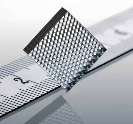
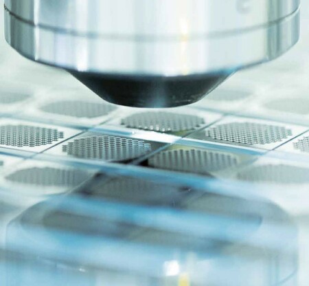
Focuslight imprint capabilities give customers the flexibility they need to design demanding structures for their applications, including freeform micro-optics, high fill factors (up to 100%) and mixes of concave and convex shapes. This technology has been deployed in high volume manufacturing for the automotive industry, making it a good solution for cost-sensitive markets while benefiting from stable processes. Using the latest equipment developed by our parent company SUSS MicroTec, we can replicate even the most demanding lens shapes at cost competitive prices.
Offering Specifications
Optical & material requirements (extraction; may differ depending on application)
- Refractive structures (stochastic and periodic)
- Diffractive and hybrid on special demand
- Microlens array sizes 2 mm to 200 mm
- Optical lens size < 3 mm
- Lens sag < 500 µm
- Ra roughness <15 µm
- Form irregularity <100 nm
- Edge slopes <40°
- 3D-curved substrates
- Usage of automotive certified materials


