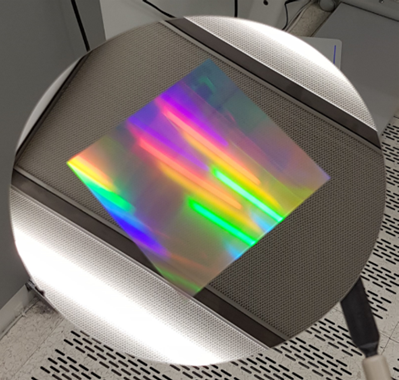
NanoImprint at wafer-scale
-
Offering type ?
PRODUCT:
Component or system, which is commercialized. It is available for ordering multiple pieces and liability is assumed by the provider/seller. Necessary certification of the product was obtained (e.g. CE certification). The product sheet and/or conditions of use are defined.
PROTOTYPE:
Component or system, which has been successfully tested under real or real-like conditions. The prototype is not commercialized as the main purpose is to use it for demonstration and experimentation, including user and market acceptance.
TECHNICAL SERVICE:
Tools and processes and its combination, which are necessary to prepare and test prototypes or products.
- Service
-
Market
- AR/VR/MR
- Automotive
- Consumer Products
- Decoration & Luxury
- Healthcare & Life Sciences
- Imagers & Displays
- Lighting
-
Manufacturing Pillar
- Wafer-scale
-
Technology
- UV-NIL replication
Organisation
Offering Description
CEA-Leti have capability to perform NanoImprinting at wafer-scale.
The technology used to perform this replication is soft UV-NIL. It allows to pattern Si or glass wafer from a first master wafer and keep the same polarity. The associated materials and equipment allow to reach an high throughput of 60 wafers per hour.
Size of patterns replicated are from micrometers to nanometers. It is possible to replicate 2D shape, 3D shape or freeform with angle below 90°. The resist used for replication could be change to have the specific refractive index needed.
Offering Specifications
Performances
- Min replicating patterns width 45nm
- WtW uniformity on 25 wafers s < 1% for sub50nm
- Intra-wafer CD uniformity s < <2% for sub50nm (< 1% bigger structures)
- Overlay ±3µm (~±1µm distortion)
- Defectivity count <10 def./cm²
- High aspect ratio (>5)
Others capabilities
- Si or Glass wafer
- Large surface
- 2D, 3D shape and freeform
- Different resist RI available


