Origination – MicroLens Array
-
Offering type ?
PRODUCT:
Component or system, which is commercialized. It is available for ordering multiple pieces and liability is assumed by the provider/seller. Necessary certification of the product was obtained (e.g. CE certification). The product sheet and/or conditions of use are defined.
PROTOTYPE:
Component or system, which has been successfully tested under real or real-like conditions. The prototype is not commercialized as the main purpose is to use it for demonstration and experimentation, including user and market acceptance.
TECHNICAL SERVICE:
Tools and processes and its combination, which are necessary to prepare and test prototypes or products.
- Masters (origination)
-
Market
- AR/VR/MR
- Automotive
- Consumer Products
- Decoration & Luxury
- Healthcare & Life Sciences
- Imagers & Displays
- Lighting
-
Manufacturing Pillar
- Wafer-scale
-
Technology
- Dry Etching
- Wet Etching
Organisation
Offering Description
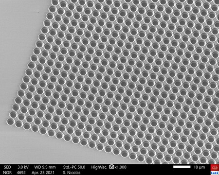
MicroLens Array master manufactured by CEA-Leti is made of Si and SiO2.
Manufacturing is based on standard lithography associated to dry and wet etch to obtain the final shape on demand.
It is associated to specific design of customer, down to 2 µm microlenses without gap. It could cover surface from some micrometer to the full wafer. The technology used guarantee uniformity over the full wafer.
Offering Specifications
Substrate and surface
- 200 mm Si wafer
- Maximum Area : full wafer
- Minimum Area : /
- Material : Si and SiO2
Features
- Minimum size
- CD : 2 µm
- Height : 1µm
- Pitch : 2 µm
- No gap
- Maximum size
- CD = 100µm
- Height : 5 µm
- Pitch : 2 µm
- Aspect ratio H/Pitch = 1/4
- Concave shape


