Tooling (electro-forming)
-
Offering type ?
PRODUCT:
Component or system, which is commercialized. It is available for ordering multiple pieces and liability is assumed by the provider/seller. Necessary certification of the product was obtained (e.g. CE certification). The product sheet and/or conditions of use are defined.
PROTOTYPE:
Component or system, which has been successfully tested under real or real-like conditions. The prototype is not commercialized as the main purpose is to use it for demonstration and experimentation, including user and market acceptance.
TECHNICAL SERVICE:
Tools and processes and its combination, which are necessary to prepare and test prototypes or products.
- Service
-
Market
- AR/VR/MR
- Automotive
- Consumer Products
- Decoration & Luxury
- Healthcare & Life Sciences
- Imagers & Displays
- Lighting
-
Manufacturing Pillar
- Wafer-scale
- Roll-2-Plate
- Roll-2-Roll
-
Technology
- Electroforming
Organisation
Offering Description
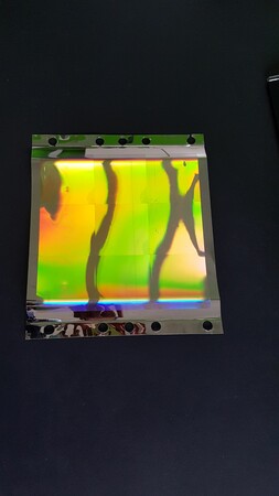
CSEM has electroforming infrastructure for small area (8’’ wafer scale, galvanisation of Ni and other metals) and large area Ni shims. The maximum size for large area Ni shims is 35×55 cm. The main application of this galvanization process is the fabrication of Ni shims from structure masters and the fabrication of 2nd (and higher) generation copies of Ni shims. Both the 1st generation Ni and – depending on the material – the original master are kept safe, while the 2nd generation copies are used for all subsequent upscaling (e.g. S&R UV-imprint) and replication processes (e.g. R2P and R2R UV imprint).
Offering Specifications
- Substrate sizes:
- Width of max 350mm
- Length of max 550mm
- Substrate thickness: 0.1 – 50 mm
- Substrate materials: Glass, polymer, metal
- Textures: from 20 nanometer up to 500 micrometer


