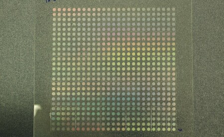
Tooling (step and repeat)
-
Offering type ?
PRODUCT:
Component or system, which is commercialized. It is available for ordering multiple pieces and liability is assumed by the provider/seller. Necessary certification of the product was obtained (e.g. CE certification). The product sheet and/or conditions of use are defined.
PROTOTYPE:
Component or system, which has been successfully tested under real or real-like conditions. The prototype is not commercialized as the main purpose is to use it for demonstration and experimentation, including user and market acceptance.
TECHNICAL SERVICE:
Tools and processes and its combination, which are necessary to prepare and test prototypes or products.
- Tooling
-
Market
- AR/VR/MR
- Automotive
- Consumer Products
- Decoration & Luxury
- Healthcare & Life Sciences
- Imagers & Displays
- Lighting
-
Manufacturing Pillar
- Wafer-scale
- Roll-2-Plate
- Roll-2-Roll
-
Technology
- Other
Organisation
Offering Description
Step&Repeat UV-imprint Lithography is a method to replicate nano- and microstructures from small sized masters onto large area substrates which form the basis for the tooling needed in roll-to-roll and roll-to-plate mass-production. CSEM has developed a S&R tool for high precision (<5 µm) upscaling of rigid small masters to (flexible) tools with 600 x 350 mm2 dimensions. The S&R upscaled tools are functional to CSEM’s combined manufacturing platform which ranges from design and origination of small master structures to replication on large areas by R2P UV-imprinting.
CSEM has an extensive network of industrial partners along the value chain up to end-users, in domains where S&R upscaling technology is expected to become key manufacturing steps for free-form optical micro-structures on larger areas.
Basic process description – In the step and repeat process, a UV crosslinkable monomer mixture is dispensed onto the substrate at the spot of the imprint. A transparent nanostructured stamp is approached to the substrate and pressed into the wet monomer mixture. Because the monomer mixture has a low viscosity the application of a moderate imprint pressure allows for obtaining a thin residual layer. After UV curing the stamp is released from the surface, leaving its nanostructure replicated in the cured polymer. The same procedure is repeated until the desired area on the substrate has been covered with the nanostructure.
Offering Specifications
- Substrate sizes:
- Width of max 350mm
- Length of max 600mm
- Substrate thickness: 0.1 – 10 mm
- Substrate materials: Glass, polymer, metal
- Textures: from 20 nanometer up to 200 micrometer


